The Microfluidic Medical Device Facility (Contact: Zhicheng Long, z1long@eng.ucsd.edu, 858-822-5663) is the latest addition to the Nano3 nano/micro-fabrication cleanroom facility. It is accessible to academic and industry users. We provide a well-equipped facility with experienced staff to allow users to independently fabricate microfluidic devices and we offer foundry or contractual fabrication services. The facility can offer several unique capabilities and services, including master mold fabrication, PDMS molding and bonding, rapid prototyping by CNC micro-milling, hot embossing and bonding, incorporation of metal electrodes, multi layer microfluidics with micropneumatic valves or Organ-on-a-Chip models, and more.

General Information
The devices we fabricate can have multiple layers, valves, electrodes; can be made with soft lithography techniques or hot embossing; can be used for a broad spectrum of applications, e.g. micropneumatic systems (micro-pumps and micro-valves); Organ-on-a-Chip; immunoassays; cell separation, sorting, counting and manipulation; droplet manipulation and digital microfluidics; optofluidics; drug screening and delivery; etc.
In our laboratories, we fabricate microfluidic platforms made of thermoplastic polymers such as COC/COP (Cyclic olefin copolymer and polymer), PC (Polycarbonate), PMMA (Poly(methyl methacrylate) or silicones (PDMS - Polydimethylsiloxane) or resins. We also developed bonding processes combining PDMS-PDMS, Glass-PDMS, COC/COP-PDMS, COC/COP-COC/COP, Glass-PDMS-PDMS, PDMS-PDMS-PDMS, COC/COP-PDMS-COC/COP.
Academic and industry users have access to our microfluidics laboratory after receiving introductory equipment training and authorization by facility staff.
The facility also provides a variety of direct services: we can fabricate molds for soft lithography or hot embossing, and we can also fabricate devices in PDMS (single or multilayer) or COC/COP (hot embossed or CNC milled).
Polydimethylsiloxane (PDMS) is a transparent silicone commonly used for biological applications due to high optical clarity, inertness, non-toxicity and high hydrophobicity.
Cyclic Olefin Copolymer (COC) is an amorphous polymer with exceptional optical properties: high transparency, low auto-fluorescence and high ultraviolet transmission. COC is generally attacked by non-polar solvents, such as toluene but shows good chemical resistance and barrier to other solvents, such as alcohols or acetone, and is very resistant to attack from acids and bases.
Equipment
The Microfluidic Medical Device Facility at Nano3 is equipped with:
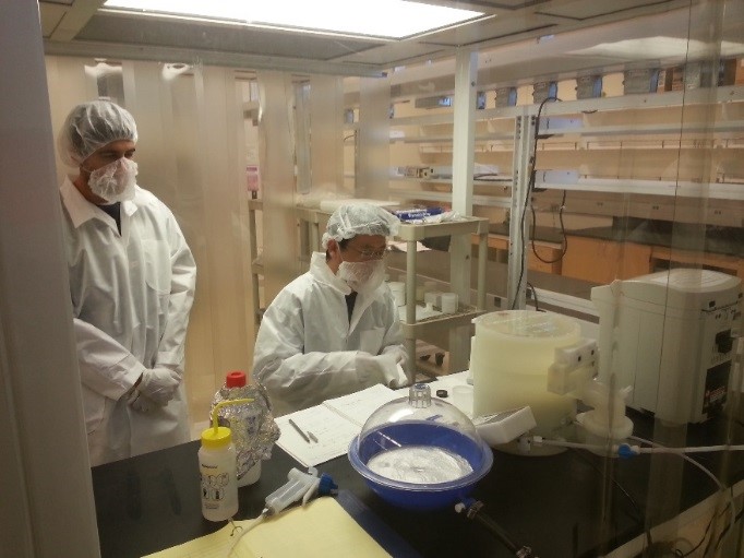
This is a clean (Class 1000 HEPA filtered) area designated primarily for PDMS processing. Available equipment includes a Thinky Mixer, Laurel Spin Coater, scale, vacuum desiccator, ozone plasma system and oven. Users may complete the entire PDMS molding process in this clean space using mold masters fabricated in the Nano3 cleanroom.
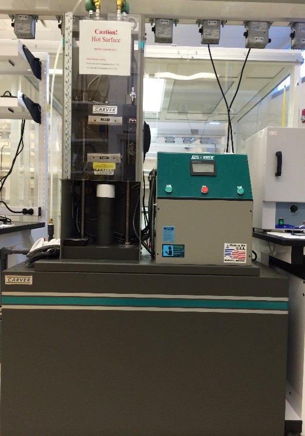
The Carver Hot Embossing system allows hot embossing and bonding of thermoplastic polymers. The top and bottom embossing plates can be heated at different temperatures, up to 200°C, and embossing pressure of up to 5tons (1000lbs minimum) can be applied. The equipment has been successfully tested with PC, PMMA, COC-COP, PTFE and PE. It can be used with silicon, epoxy resin, glass, or aluminum molds, depending on the desired feature size.
4-axis CNC micro-milling machine
Our Minitech 4 axis CNC micro milling machine (step size resolution 0.1µm) can be used for fast prototyping of molds, devices or sample holders. It can be used with polymers or soft metals (Aluminum, Copper, etc.), to precisely drill holes or micro-machine complex shapes with micro bits. Designs can be implemented using Autodesk Fusion 360, Solidworks and Mastercam software.
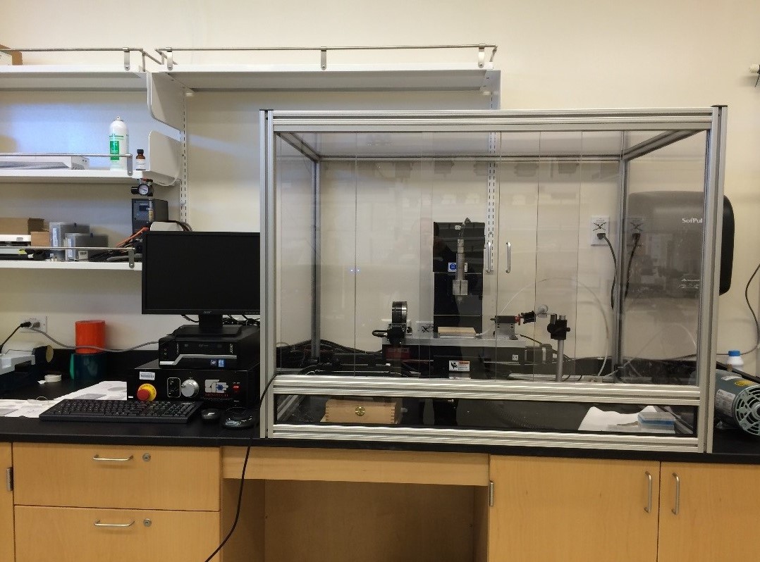
Microfluidics testing workstation
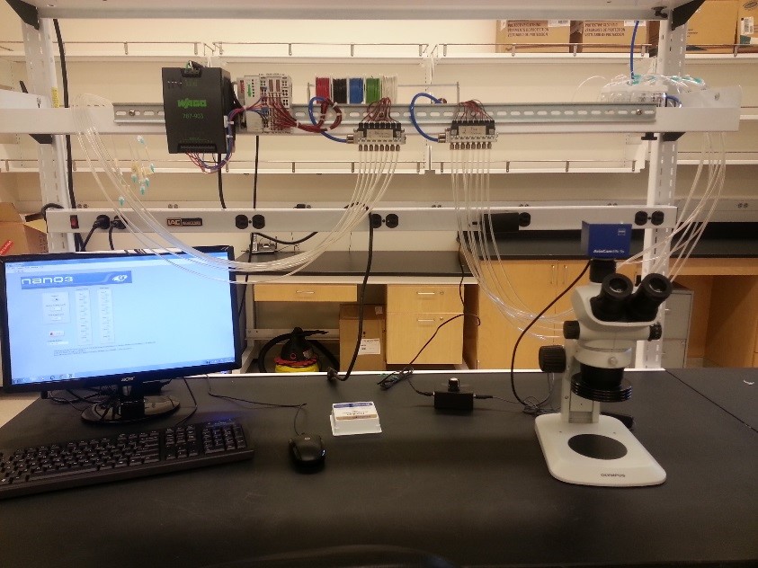
The microfluidics workstation is set up for validation and screening of microfluidic devices. Materials supply and control line N2 pressures can be independently adjusted. 16 independent flow channels are available with 8m/s response time. The pressure range is between 0 and 50psi (0 and 345kPa) for pneumatic microvalve control and between 0-2psi (0-13.8kPa) for pressure-driven microfluidic flows.
The system can be used in manual mode or can be programmed to perform cycles or more complex routines.
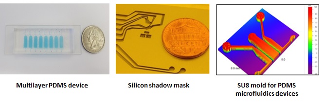
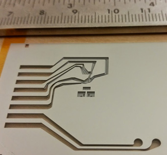
Silicon Shadow Mask
Shadow masks are commonly used to pattern devices without any lithographic step. Realized, usually, in a thin sheet of metal the thickness of these masks (at least 120-150µm) allows to pattern only flat surfaces and not channels or cavities. This has been seen by the scientific community as a huge limitation for many microfluidic applications.
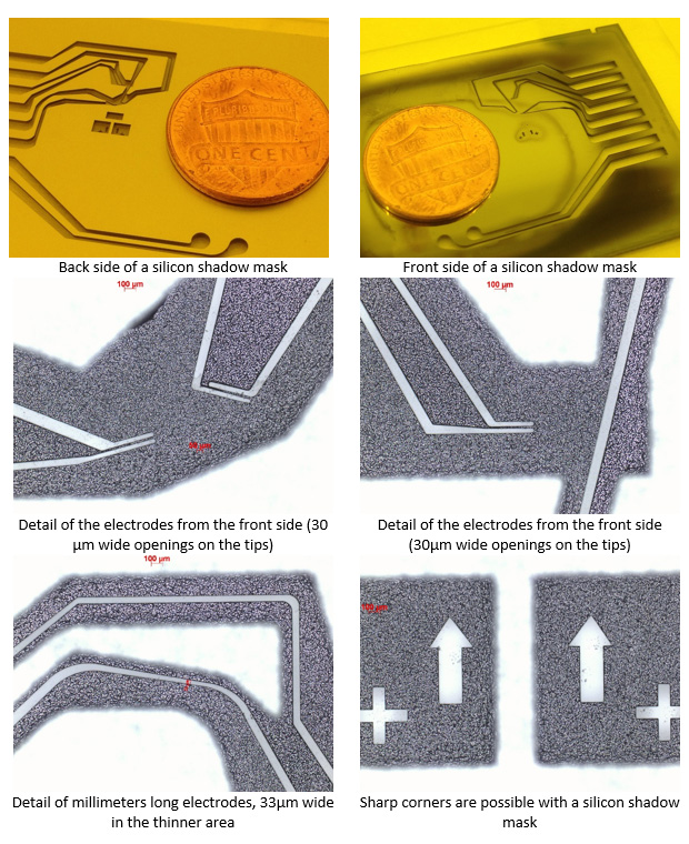
At Nano3 Biomedical Devices and Platforms, we developed an innovative process to realize silicon shadow masks with a minimum thickness of 50 µm.
Pattern
Since we use traditional photolithography, the resolution of the shadow mask depends on the mask used for the pattern. Typically can resolve 30 µm open features within about +/-1microns.
To prevent the collapse of long bridges (in the millimeters range) and to guarantee structural integrity, the smallest space between openings should be not less than 30 µm.
Dimension
We realize our silicon based shadow masks on 4” wafers.
Price
Ask us for a quote.
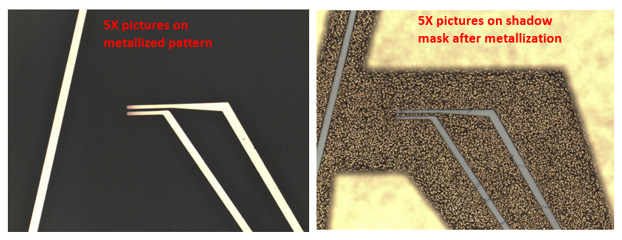
Metallization Examples:
Facility Usage
Facility
In our fully equipped laboratory users can design, fabricate and test their own devices, taking advantage of a state of the art cleanroom, dedicated Class 1000 PDMS clean space, hot embossing system, CNC micromill, and microfluidics multifunctional workstation.
Foundry
We also provide a foundry service at different levels. We can help the users from the design of their microfluidic devices to the realization of the final chip.
We have developed processes that allow metallization of microfluidic circuits, multilayer microfluidics with active (valve/pump) components in PDMS or COC; and bonding techniques that can be transferred to different materials. CNC micromachining equipment permits fast prototyping and fabrication of molds or devices with micrometric features.
Mask and device design general guidelines
When you design your chip you must be aware that there are different requirements for different devices: if you are planning to realize a mold for soft lithography (PDMS), your mold is going to be a silicon wafer with SU8 patterns; while if you are looking to a mold for hot embossing, you may want to choose between silicon or aluminum.
When you design your mold, all devices must have a border indicating the external edges of the chip and where it should be diced. The recommended size of the mold is 4" in diameter.
The AutoCAD file containing your project must be saved in .dwg format (earlier than Autocad 2013); make sure that the internal units of your file are set up properly (Length Type: Decimal, Length Precision: 0.0000, Drag-and-drop Scale: Microns) and each single layer of your device is drawn in a separate layer. Remember to leave at least 10mm around the mold perimeter and draw your features with closed polylines, use the command overkill to remove overlapping lines; and verify that polylines and regions do not cross each other.
Alignment marks must be present in your design to allow a proper alignment of different layers of your mold. Several alignment marks must also be present in each region of the chip to align the different layers prior bonding.
Remember also to label the mask with name, date, project name and version number.
Some additional information about standards for your chip design:
- Chip size: Microscope slide (75x25mm) thickness max 5mm preferably less than 2mm
- For PDMS devices, features density: to guarantee a the bonding, two adjacent channels should possibly be separated by twice their width (not less than 200µm) and no more than 50% of the total area should be covered by structural elements
- Electrodes: 50-200nm sputtered Au or Pt; access to the electrodes through chips holes or side connectors
- Distance between devices: 2mm minimum
- Through holes and Connections I/O: Minimum diameter 500µm, connected with mini-luer fittings
- Minimum radius of curvature: At intersecting features r = 40µm
- Minimum feature size for lithography: ~1.0 μm; Maximum thickness of SU-8 patterns: ~ 200 μm (maximum aspect ratio is 1.5)
FAQs
- Can I make my own devices?
- What are the steps to realize a PDMS device?
- What are the steps to realize a COC hot embossed device?
- How can I get a micro-machined prototype?
- What kind of mold do I need to hot emboss?
- What's the minimum feature size I can hot emboss?
- What's the maximum working temperature of the Carver hot embossing press?
- What's the maximum dimension of the mold for the hot embossing press?
- Why should I use COC as hot embossed substrate?
- Can my final device have electrodes?
- Where can I test my devices?
- Do I need any treatment before using the molds for soft lithography?
You may independently use the PDMS clean space, hot embossing machine, CNC micromilling system and microfluidics testing system after initial user training/authorization by staff.
Design your mask; realize the mold (Silicon wafer with SU8 patterns); perform an anti-adhesion treatment to your mold; pour PDMS on the mold and cure it; bond it to PDMS or a glass substrate. (to learn more, attend our PDMS Molding Short Course).
Design your mask; make your mold; use the hot embossing press to create a replica of your device; bond it if needed.
Contact our staff to discuss your device design.
You can use silicon, epoxy resin or aluminum molds. You can independently fabricate these in the main Nano3 cleanroom or use our mold fabrication services to have them made for you.
The feature size depends on the features of your mold. We have successfully embossed features as small as 200nm. For smaller features you should use nano-imprint lithography system (EVG620) and contact our specialist (Dr Lu xklu@ucsd.edu).
The system must be operated below 200°C.
The hot plates are 5 inches by 5 inches, the mold should fit that area.
Cyclic Olefin Copolymer (COC) is an amorphous polymer with exceptional optical properties: high transparency, low auto-fluorescence and high ultraviolet transmission. COC is generally attacked by non-polar solvents, such as toluene but shows good chemical resistance and barrier to other solvents, such as alcohols or acetone, and is very resistant to attack from acids and bases.
Yes, if the device is made of COC the best technique is to use a sputtering process (i.e. Au) and a shadow mask to realize electrodes on your device. We have developed a procedure to realize shadow masks for features in the tens of micrometer range, with spacing between electrodes also in the tens of micrometer range, and we can pattern inside microfluidic channels. If you are fabricating PDMS devices, electrodes can be easily patterned on the glass substrate where the PDMS is bonded but not inside of the channels.
We have set up a workstation where it is possible to test up to 16 channels at the time. The N2 pressure in each channels is controlled by programmable software and you can use them to control pneumatic microvalves or turn them into pressure-driven microfluidic pumps.
We suggest to treat the wafers with a surfactant. We provide Fluoro Octo Trichloro Silane (FOTS) which silanizes the surface to prevent adhesion of PDMS to your mold, keeping it cleaner and facilitating the de-molding process.